The Art of RF Wirebonding
It was summer 2019 when I first got introduced to wirebonding. It is not like I did not know what the term meant, but that was the first time I got to actually operate a bonder machine, and I managed, within two hours of being trained by a co-worker, to damage my first wedge tool. Good times (he was not happy about it, in case you were wondering 😅). I learned a lot about wirebonding after that, especially for RF, since that was the whole reason I was doing it: chip integration. It was my master’s thesis [1] to do everything, from researching wirebonds, to making them, to simulating, modeling, and measuring them. I honestly loved that time. It was frustrating to thread a 25 µm wire through a wedge tool from behind, without even seeing the hole, and to learn how to keep my hands from shaking and handle tweezers gently. But it was so rewarding, and ever since I have an unbelievable respect for anyone who does this for a living. You would be amazed how much wirebonding is still done in electronics. It can be automated, but a lot of RF wirebonding is still manual or semi-automatic, and even then it requires a person with experience, steady hands, and patience… a lot of it 😉.
So I want to revisit what I did back then and explain wirebonding for RF. That period was actually my first time doing many things beyond wirebonding, like working with mmWave frequencies, operating an on-wafer probe station, and learning about de-embedding, among many others. I cannot write down everything I learned, but I want to at least explain how I came to understand wirebonds and what my conclusion was regarding RF integration.
For those interested, I have a repository on inductance calculation using Neumann’s integral that was used for the inductance calculation of the considered wirebonds: https://github.com/ZiadHatab/neumann-self-and-mutual-inductance
Wirebond or Bond-wire?
The first thing that confused me was the naming, because no one had a convention. Many people say “bond-wire” for the wire itself and “wire bonding” for the process. I, on the other hand, just learned it as “wirebond” for the wire and “wirebonding” for the process, and it still makes more sense to me this way, because I never have to remember when to flip the word around. I know it is semantics, but I thought I should point it out upfront so we are on the same page for the rest of the post.
What Is a Wirebond, and Why Should You Care?
A wirebond is exactly what it sounds like: a thin metal wire that welds two pads together to make an electrical connection, e.g., chip-to-chip or chip-to-substrate. The wires are usually gold or aluminum, and the standard diameter is 25 µm (I used 17 µm and 50 µm as well). Now look at the photo below, a shot of real gold wirebonds catching the light, and try to appreciate that every one of those wires was placed by a manually guided machine. The person guiding it happened to be me, and I am very proud of this picture 😊.
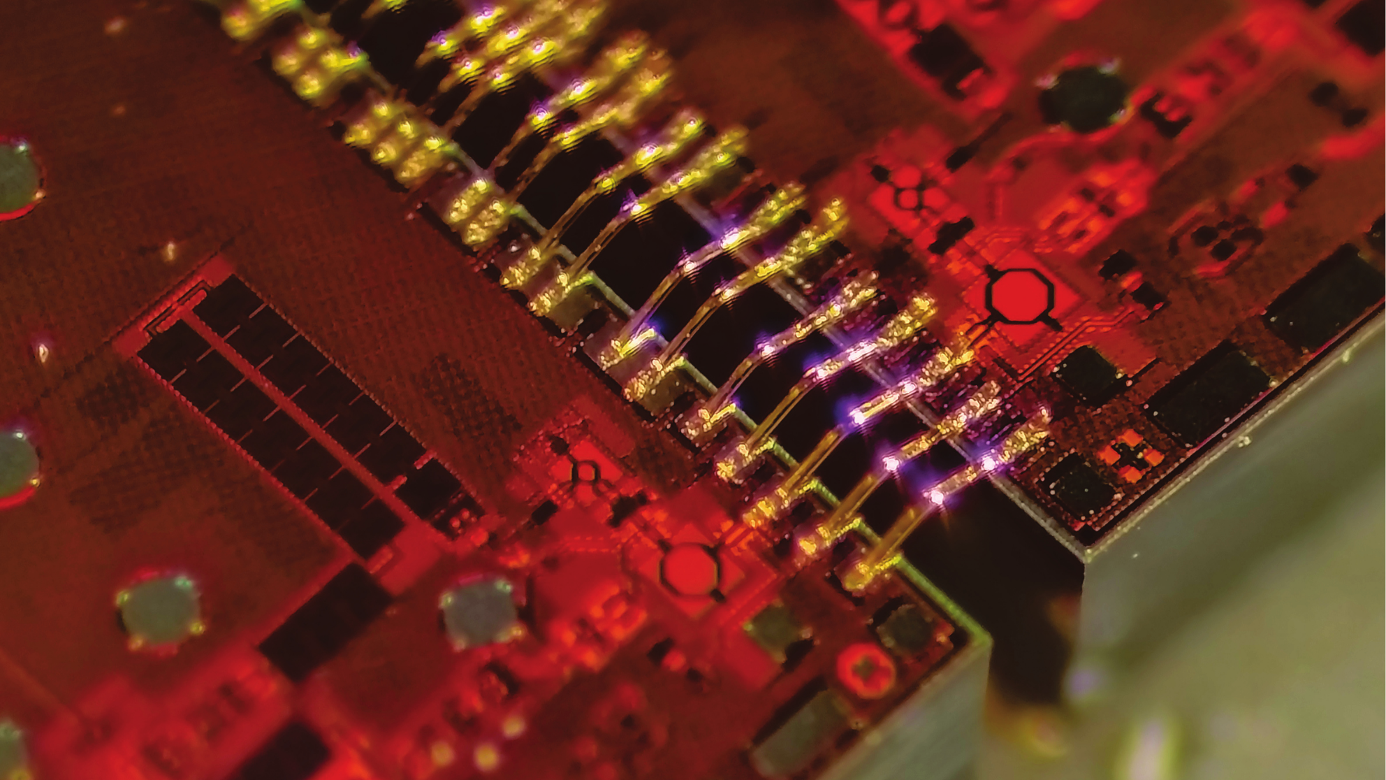 Fig. 1.: A macro photograph of gold 25 µm wirebonds; this was the cover image of my thesis [1].
Wirebonding is one of the oldest and most mature interconnect technologies in electronics, and it is everywhere. Open up almost any chip package and there is a good chance the die is connected to the outside world through wirebonds. In this post, though, the context is heterogeneous integration: the idea of placing several bare chips side by side on a common substrate and connecting them so the whole thing behaves as one system. The motivation is both economics and engineering. Cramming every function into one large System on a Chip hurts the fabrication yield and forces everything onto one process, whereas splitting the system into smaller specialized chips lets each be made in the technology that suits it best (and lets you reuse existing chips in new designs). Sometimes there is no choice at all: no single semiconductor process can deliver the required performance for every function, so at the end of the day you are bound to mix technologies. When the chips sit next to each other on an interposer in a planar arrangement, it is called 2.5D integration; the interposer routes the signals between the chips, and through-silicon vias carry them down to the package. The two most common ways to make the short die-to-die connections are wirebonds and flip-chip, illustrated below.
 Fig. 2.: Two interconnect options for 2.5D integration: wirebonds (left) and flip-chip (right).
Flip-chip flips the die upside down and connects its pads directly to the interposer through tiny bumps, which gives very short connections and low parasitics. It is the better performer at high frequency, but it comes with stricter design rules and a less flexible process. Wirebonds are the opposite: they add more parasitic inductance because the wire has to loop up and over, but the process is simpler, cheaper, and far more forgiving. If you already have a chip and an interposer that almost fit each other, wirebonds will bridge the gap without a redesign.
There is one more argument for wirebonds that I find underrated: measurement correlation. Bare RF chips are characterized on-wafer, with probe tips landing directly on the chip pads and the calibration reference sitting right at those tips. A wirebond (or ribbon) transition resembles that probe contact closely, so the chip performance you measured, and the models you built from it, carry over to the assembled system. On the other hand, with flip-chip the chip sits on bumps, and the interposer material interacts with the IC traces and pads. These boundary conditions were never seen by the probe measurement, so the chip in the system no longer behaves quite like the chip on the probe station. That flexibility plus predictability is why, despite flip-chip being “superior” on paper, wirebonding is still very much here to stay.
Making the Bond
Before we get to the RF side, it helps to know how the bond is actually formed, because the mechanics explain a lot of the electrical behavior later. Welding two metals needs three ingredients: heat, pressure, and a clean interface. The three classic wirebonding technologies each mix these differently [9, 10]:
Thermocompression bonding uses only heat and pressure. It needs very high temperatures (>300 °C), which many chips cannot survive.
Ultrasonic bonding replaces heat with friction, like ultrasonic welding. The tool vibrates the wire laterally at ultrasonic frequencies (tens of kHz) while pressing down, scrubbing the interface clean and welding the metals at room temperature. It typically uses aluminum wire and a flat wedge tool.
Thermosonic bonding combines the two: ultrasonic energy plus a modest amount of heat (around 120 °C). It usually uses gold wire and a ball bond, formed with a ceramic capillary tool. That said, thermosonic bonding also works with a wedge tool and gold wire.
For any bonding that uses ultrasonic energy, there are three parameters you actually tune on the machine: ultrasonic power, force, and time. Power is the key ingredient; too much destroys the bond, too little fails to clean the interface and you get a weak (or no) bond. There is a trade-off between power and force, and finding the sweet spot depends heavily on the machine, the tool, and the wire. This is exactly the “experience” part I mentioned in the intro.
Let me start with ultrasonic wedge bonding, which relies on a scrubbing action. While the wedge presses the wire onto the pad, it also vibrates it sideways at an ultrasonic frequency (around 63 kHz on the machine I used, for roughly 100–200 ms). That rapid rubbing sweeps away surface contamination and oxide and brings fresh metal into contact, so the two sides cold-weld without anything melting. The rest of the wedge cycle is simple: press and scrub the first bond, loop over to the second pad, bond it the same way, and tear the wire. My sketches below show both the scrubbing principle and the full cycle.
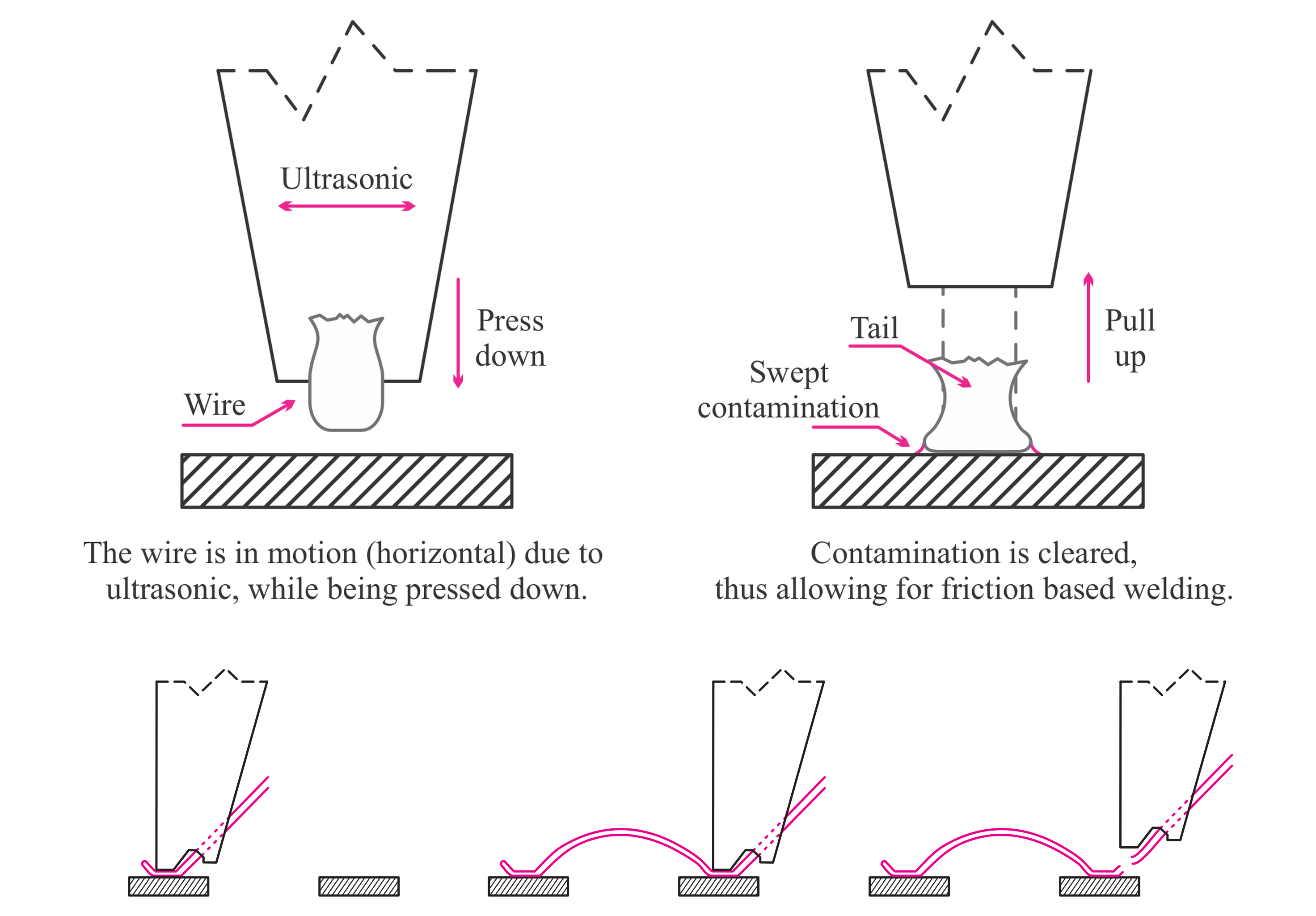 Fig. 3.: Sketch of ultrasonic wedge bonding. Top: the wire is scrubbed sideways (~63 kHz) while pressed down, sweeping away contamination for a friction weld. Bottom: the full wedge cycle, first bond, loop over to the second bond, tear the wire.
Now, add a modest amount of heat to that scrubbing and you get thermosonic bonding, the usual choice for gold ball bonds formed with a ceramic capillary. The cycle differs mainly at the start: a high-voltage spark (the electronic flame-off, EFO) melts the wire tail into a free-air ball, the capillary presses that ball onto the first pad, loops up and over to the second pad, forms the second bond, and tears the wire, leaving a fresh tail for the next cycle.
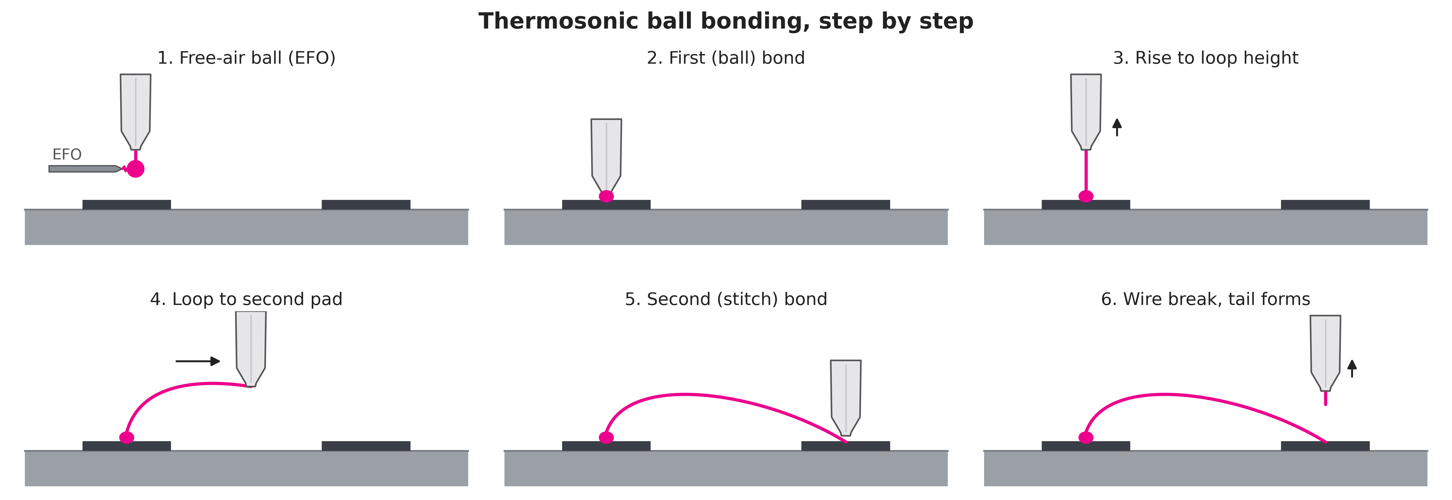 Fig. 4.: The thermosonic ball bonding cycle, from the free-air ball formed by the flame-off, through the first (ball) bond, the loop, the second bond, and finally the wire break that leaves a tail for the next ball.
In my thesis I used wedge bonding with 25 µm gold wire, on a semi-automatic machine that was motorized only in two axes (up-down and back-forth). There was no sideways motorization, so I had to keep the tool perfectly straight while looping to the second bond; if you drift sideways, the wire slips out from under the wedge and the bond fails. Ball bonding does not have that constraint (the capillary is symmetric, so it can bond in any direction), which is one reason automatic ball bonders are faster than wedge bonders. The picture below shows the actual machine I used back at TU Graz:
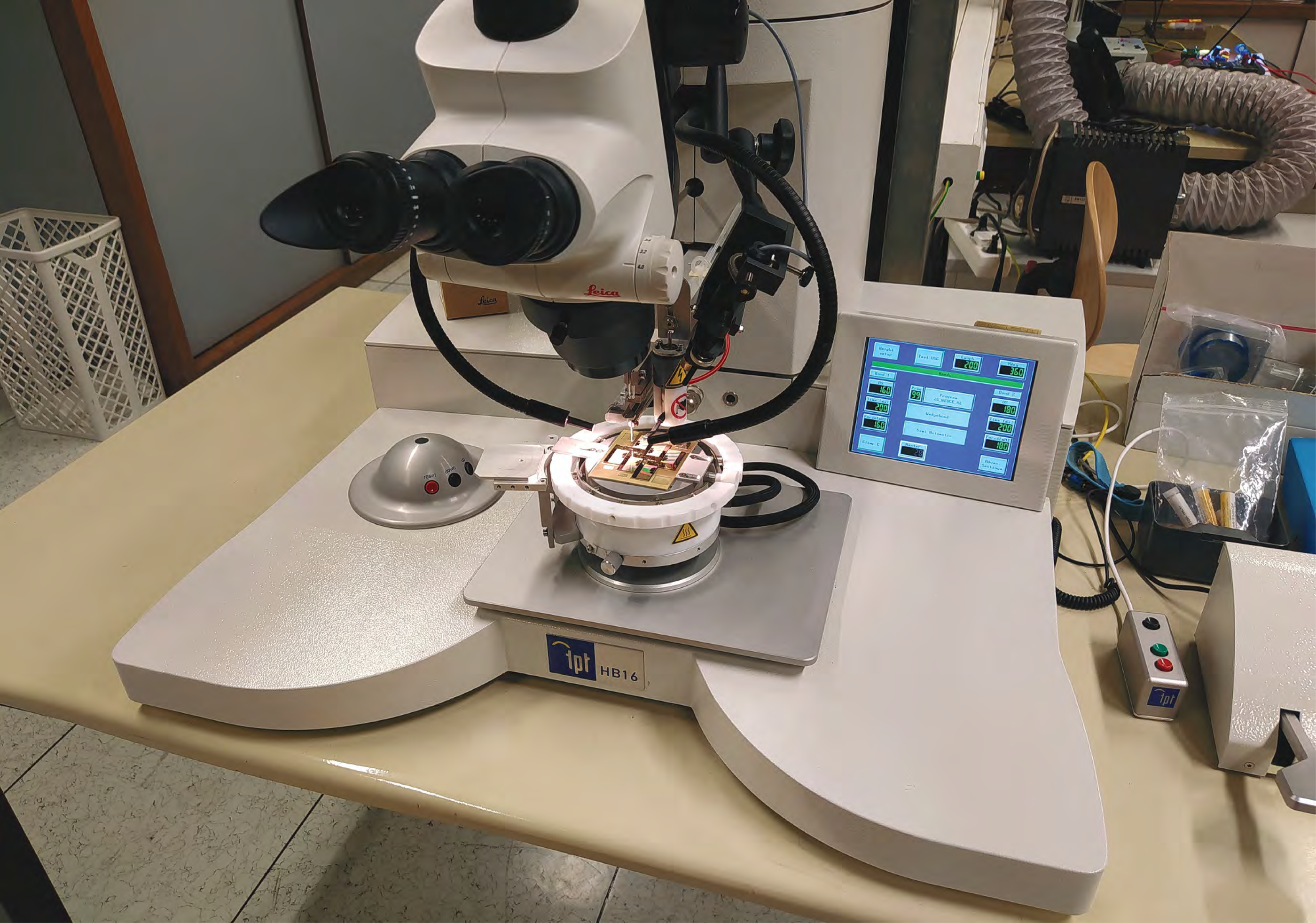 Fig. 5.: The semi-automatic bonder I used (TPT HB16) at TU Graz.
Forming the Loop
The arched shape of a wirebond is not arbitrary; it is drawn out by the motion of the tool, and I made my own sketches back then to reason about it. After the first bond, the wedge pulls straight up (the vertical pull) and then drags sideways toward the second pad (the horizontal drag), feeding out wire as it goes. The length of wire left hanging in the air is, at most, the hypotenuse of those two motions:
\[l \approx \sqrt{(\text{vertical pull})^2 + (\text{horizontal drag})^2}. \label{eq:1}\]The tool then comes back down onto the second pad, and the fed-out wire settles into the arch we recognize as a wirebond.
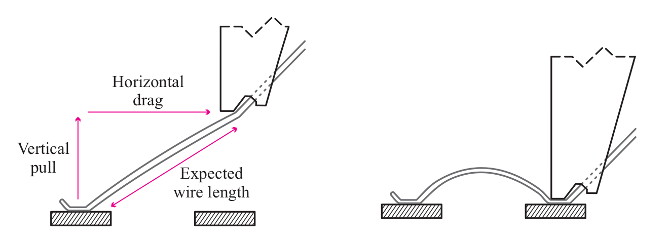 Fig. 6.: My sketches of loop formation. Left: the tool motion that sets the wire length, a vertical pull then a horizontal drag. Right: the wire settling into its loop as the wedge lands on the second bond.
This little bit of geometry matters more than it looks. The loop gives the wire mechanical stress relief, but it also makes the wire longer than the straight pad-to-pad distance, and (as the next section shows) length is inductance. It also works in reverse: if I know the tool motion, I know the wire length, and from the length I can reconstruct the loop shape. That last point is exactly what we use when we model the wire later.
The RF Problem: It Is All Inductance
Now to the reason RF engineers lose sleep over wirebonds. A wire carrying current is an inductor, and at mmWave frequencies that inductance is anything but negligible. The handy rule of thumb, which every packaging engineer knows, is:
A wirebond has roughly 1 pH of inductance per 1 µm of length.
So a 400 µm wire is about 400 pH. As we will see later, this rule slightly overestimates the real value, but it is a great estimate to keep in mind. Now, why does a few hundred pH matter? Let’s model the wire as a simple series inductance $L$ between two 50 Ω ports and look at how much power actually makes it through. The transmission coefficient is
\[S_{21} = \frac{2Z_0}{2Z_0 + j\omega L}, \label{eq:2}\]where $Z_0 = 50\,\Omega$ and $\omega = 2\pi f$. The plot below sweeps $L$ from 0 to 1 nH at three frequencies.
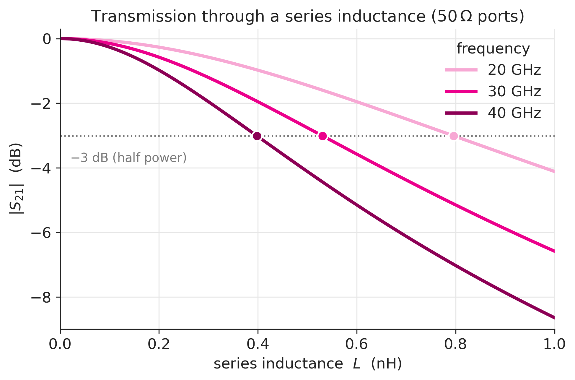 Fig. 7.: Transmission through a series inductance between two 50 Ω ports. Markers show the −3 dB (half-power) point at each frequency.
Read off the 30 GHz curve: only about 0.53 nH, which is roughly 500 µm of wire, is enough to cut the transmitted power in half (−3 dB). At 40 GHz you hit that same −3 dB point at just 0.4 nH. In other words, at these frequencies a wire that is a fraction of a millimeter too long can single-handedly become the bottleneck of your whole link. This is why, if you remember one sentence from this post, make it this: keep your wirebonds as short as physically possible. (Unless you treat them as transmission lines 🤓, but more on that later.)
Fighting the Inductance
Keeping wires short is the first and most important lever, but there is only so much you can do; the chips have a certain thickness, the pads sit at a certain place, and the wire needs a loop for mechanical stress relief. Luckily, the industry has developed a few more tricks.
Ribbon Bonds
A ribbon bond is a wedge bond with a flat, rectangular wire instead of a round one. Why does that help? At high frequency the current flows on the surface of the conductor because of the skin effect, so what matters is the surface area (the perimeter of the cross-section), not the bulk. Compare a 25 µm round wire against a 50×20 µm ribbon, per unit length:
\[A_\mathrm{wire} = \pi \times 25 = 78.5\,\mu\mathrm{m}^2/\mu\mathrm{m}, \qquad A_\mathrm{ribbon} = 2(50 + 20) = 140\,\mu\mathrm{m}^2/\mu\mathrm{m}. \label{eq:3}\]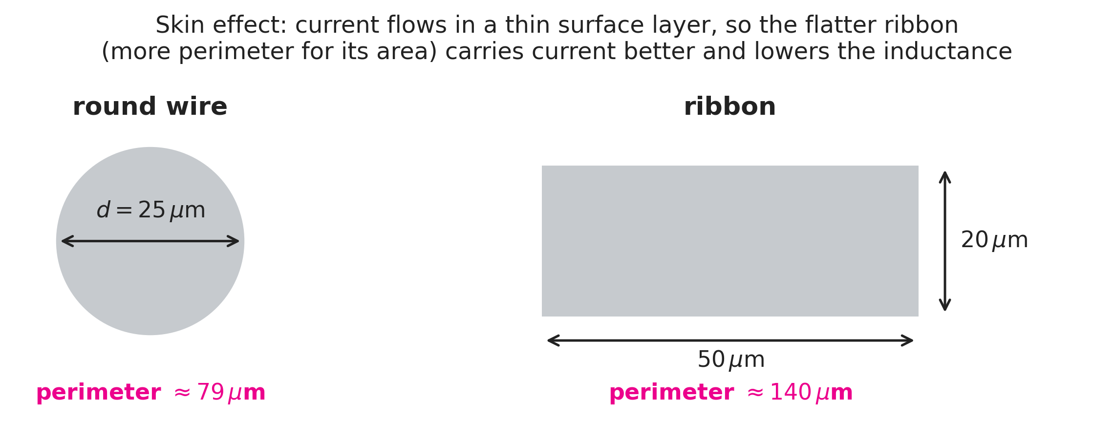 Fig. 8.: Sketch of the cross-section perimeters: the flat ribbon exposes almost twice the surface of a round wire of comparable size.
The ribbon offers almost twice the surface, hence lower inductance, and it also loops with less mechanical stress because it is wide relative to its thickness. Ribbons almost always beat round wires in RF applications; the catch is that the tooling and the fine-ribbon manufacturing are more demanding.
Fine Pitch and the GSG Configuration
The second lever is geometry. If you place the return-current path (ground) right next to the signal wire, the two carry opposite currents, and their mutual inductance reduces the total loop inductance. The tighter the loop, the lower the inductance. This is where fine pitch bonding comes in: it lets you pack bonds close together and even put several wires on one pad.
RF chips already adopt this by design, because they typically use GSG (Ground-Signal-Ground) pads. If we bond them in a GSG arrangement, with a ground wire on each side of the signal wire, we get a short, well-defined return path and strong mutual coupling that pulls the loop inductance down, while also giving a controlled characteristic impedance [7]. This GSG wirebond configuration is essentially what the rest of this post is about.
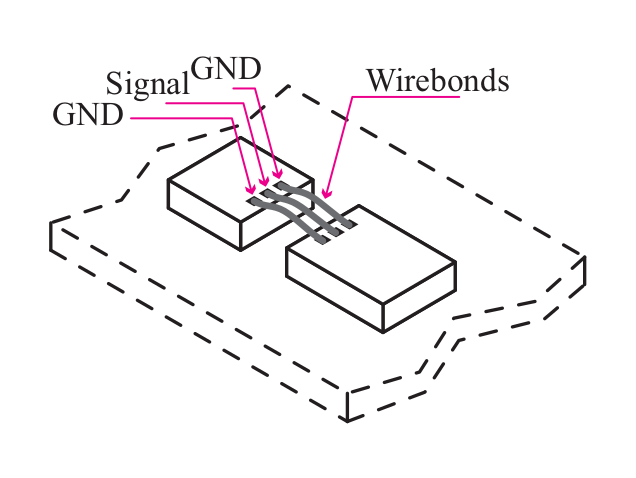 Fig. 9.: GSG wirebonds: a signal wire flanked by two ground wires.
Modeling Wirebonds
Before building anything, you want to predict how a wirebond will behave. Full 3D electromagnetic (EM) solvers can do this accurately, but they are slow and often overkill. Most of the time, engineers approximate the wire with a lumped-element model: a series inductance and resistance, plus some capacitance to nearby ground [3, 12]. Let me build this up from the simplest case.
The Straight Wire
Even though a perfectly straight wirebond is basically impossible to make (there is always a loop), the straight-wire case is the right place to start, and it is a decent approximation for short chip-to-chip bonds. Consider a floating wire with no ground nearby, so we only need the series inductance and resistance. The partial self-inductance of a round wire of length $l$ and radius $r$ is [3]
\[L = \frac{\mu_0}{2\pi}\, l\left[\sinh^{-1}\!\left(\frac{l}{r}\right) - \sqrt{1 + \left(\frac{r}{l}\right)^2} + \frac{r}{l}\right], \label{eq:4}\]where $\mu_0$ is the vacuum permeability. For $l \gg r$ this simplifies to the more familiar form
\[L \approx \frac{\mu_0}{2\pi}\, l\left[\ln\!\left(\frac{2l}{r}\right) - 1\right]. \label{eq:5}\]Equations \eqref{eq:4} and \eqref{eq:5} give the external inductance, which is what you see at high frequency because the skin effect pushes the current to the surface. The internal (“DC”) inductance dies off quickly with frequency, since the skin depth $\delta = 1/\sqrt{\mu_0\pi\sigma f}$ shrinks as frequency rises. The DC resistance is just the familiar formula
\[R_\mathrm{DC} = \frac{l}{\sigma A}, \label{eq:6}\]with $\sigma$ the conductivity and $A$ the cross-section. How good are these formulas? Below is a comparison against a quasi-static EM simulation (Ansys Q3D) for a 25 µm gold wire, sweeping the length. The analytical curve and the simulation sit right on top of each other.
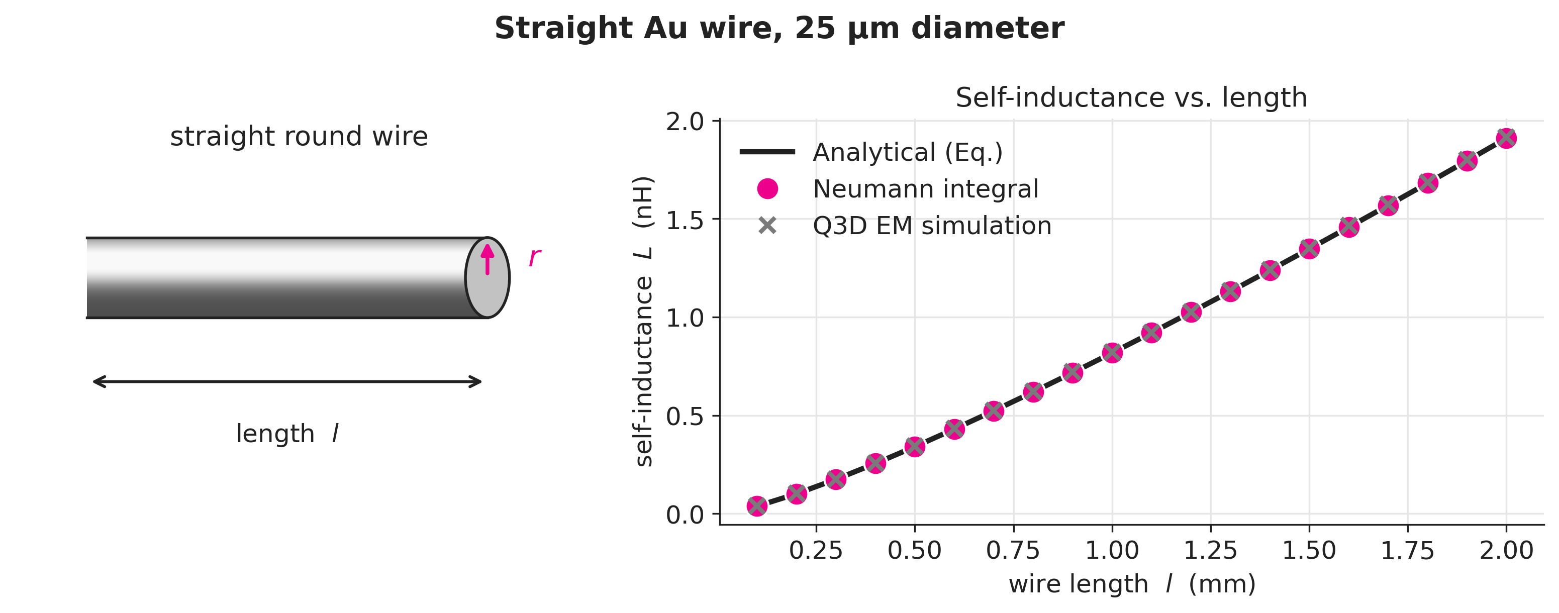 Fig. 10.: Partial self-inductance of a straight 25 µm gold wire. The closed form (Eq. \eqref{eq:4}), the Neumann integral (computed with the library linked below), and the Q3D EM simulation all land on the same curve.
Notice the inductance is a bit below the “1 pH per µm” rule; e.g., around 500 µm gives roughly 400 pH, not 500 pH. The rule of thumb is intentionally an overestimate, which is fine for a quick sanity check.
The Curved Wire: Bézier Curves and the Neumann Integral
Real wirebonds loop, and a loop is harder to pin down than a straight wire. To compute its inductance we need two things: a way to describe the shape, and a way to integrate the inductance along it.
The established way to describe the shape is to approximate the loop with a handful of straight segments. The JEDEC standard JESD59 does exactly this, breaking the wire into three or four straight pieces [4], and it is what most engineers reach for. I spent a fair bit of the thesis on this and drew my own sketches to think it through. It is simple and accurate enough at low frequency, but it has two weaknesses: you need a reference image (or a set of assumptions) to place the segments in the first place, and the sharp corners are only an approximation of a smooth arc, and the error starts to matter as the frequency climbs.
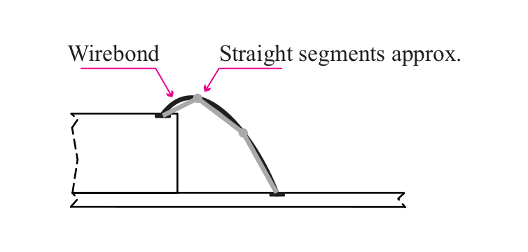 Fig. 11.: The common approach: approximate the smooth loop with a few straight segments.
I wanted something smoother and self-contained, so I reached for a Bézier curve, the same parametric spline used in vector graphics. A quadratic Bézier curve is defined by two endpoints $(x_0,y_0)$, $(x_2,y_2)$ and one control point $(x_1,y_1)$:
\[\begin{aligned} x(t) &= (1-t)^2 x_0 + 2(1-t)t\, x_1 + t^2 x_2,\\ y(t) &= (1-t)^2 y_0 + 2(1-t)t\, y_1 + t^2 y_2, \end{aligned}\qquad t\in[0,1]. \label{eq:7}\]With just those three points, a quadratic Bézier can mimic a whole zoo of realistic wire loops. The neat part is that if you know the pad locations (endpoints) and the wire length, you can back out the control point, so you can reconstruct a plausible loop shape even without a side-view photo of the actual bond. And the wire length itself is not mysterious: it comes from the bonding mechanics, the vertical-pull-and-horizontal-drag of Equation \eqref{eq:1}.
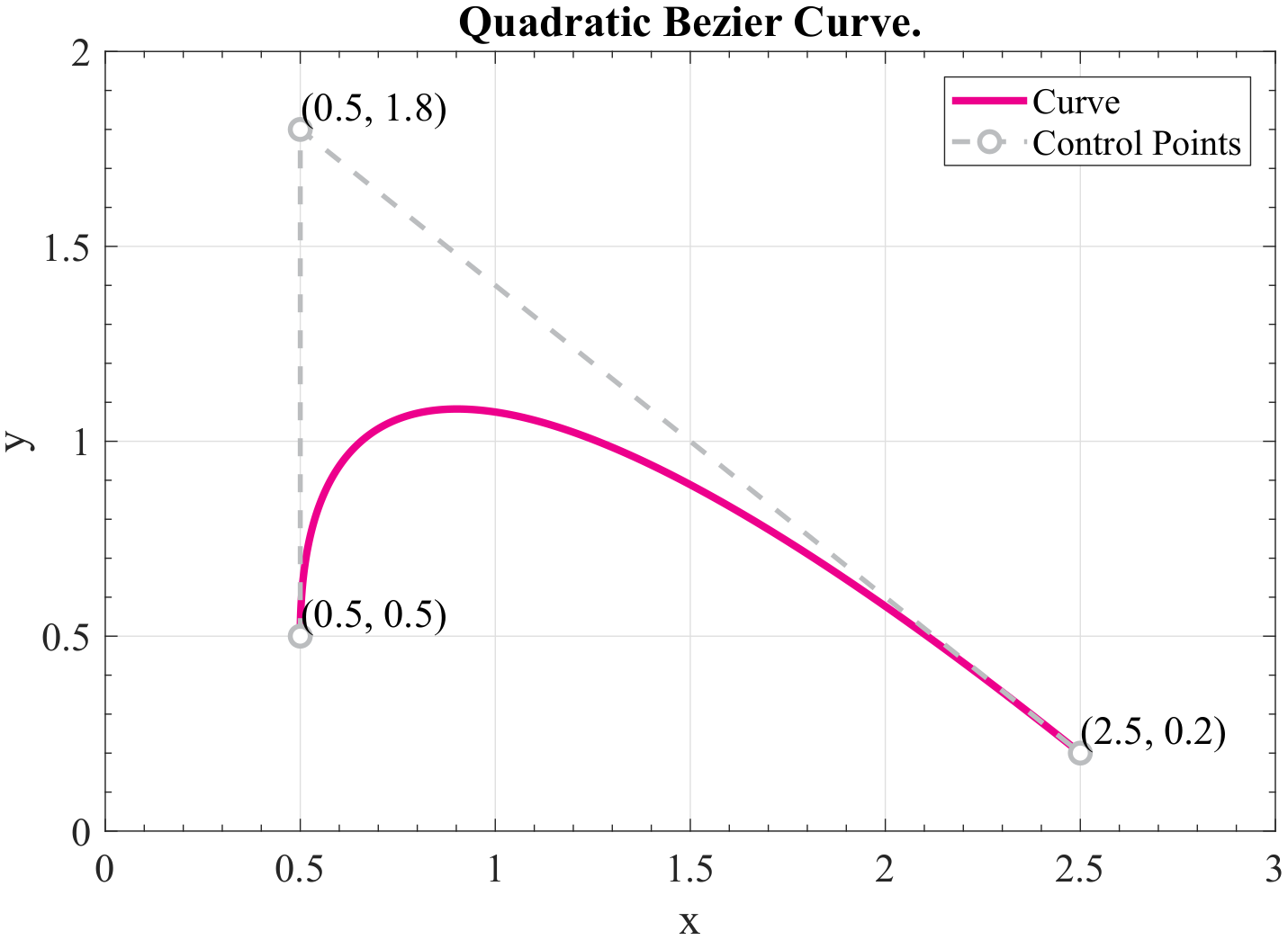 Fig. 12.: A quadratic Bézier curve, defined by two endpoints and one control point.
Once we have the shape, the inductance comes from the Neumann integral, which gives the mutual inductance between two filamentary wires of arbitrary shape [3]:
\[M = \frac{\mu_0}{4\pi}\int_{l_2}\int_{l_1} \frac{d\mathbf{l}_1\cdot d\mathbf{l}_2}{R}, \label{eq:8}\]where $R$ is the distance between the two line elements $d\mathbf{l}_1$ and $d\mathbf{l}_2$.
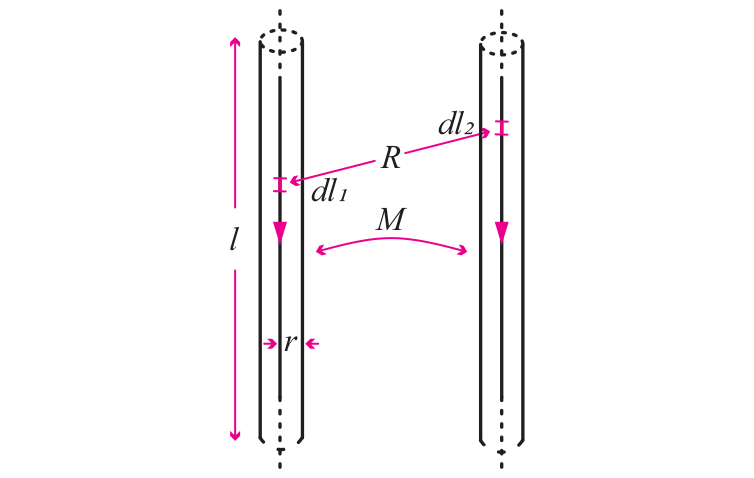 Fig. 13.: The Neumann integral computes the mutual inductance of two arbitrary wire paths.
The same integral gives the partial self-inductance of a single wire, if you let the two paths coincide. There is a subtlety: you cannot literally integrate a path against itself, because then $R = 0$ and the integral blows up. The trick is to put one path on the wire’s central axis and the other on its surface (separated by the radius $r$), which is exactly the full-skin-effect assumption:
\[L = \frac{\mu_0}{4\pi}\int_{l'}\int_{l} \frac{d\mathbf{l}'\cdot d\mathbf{l}}{R}. \label{eq:9}\]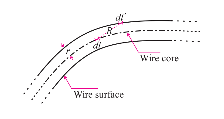 Fig. 14.: For self-inductance, one path runs along the wire axis and the other along its surface.
This is powerful: give me any wire shape as a set of 3D points (a Bézier curve, a coil, whatever) and I can compute its self- and mutual inductance numerically, no closed form required. I wrote a small Python library that does exactly this; you can find it here: neumann-self-and-mutual-inductance. It handles straight wires, wirebonds over ground planes, GSG configurations, and even solenoids and conical coils, all validated against closed-form results and measurements.
It also makes a point that the “1 pH per µm” rule is not the full story: inductance is not set by length alone, the shape matters just as much. The figure below takes four wires of the exact same length and diameter and only changes the shape. The self-inductance varies by nearly a factor of two, because folding the wire back on itself lets the anti-parallel currents cancel part of each other’s flux.
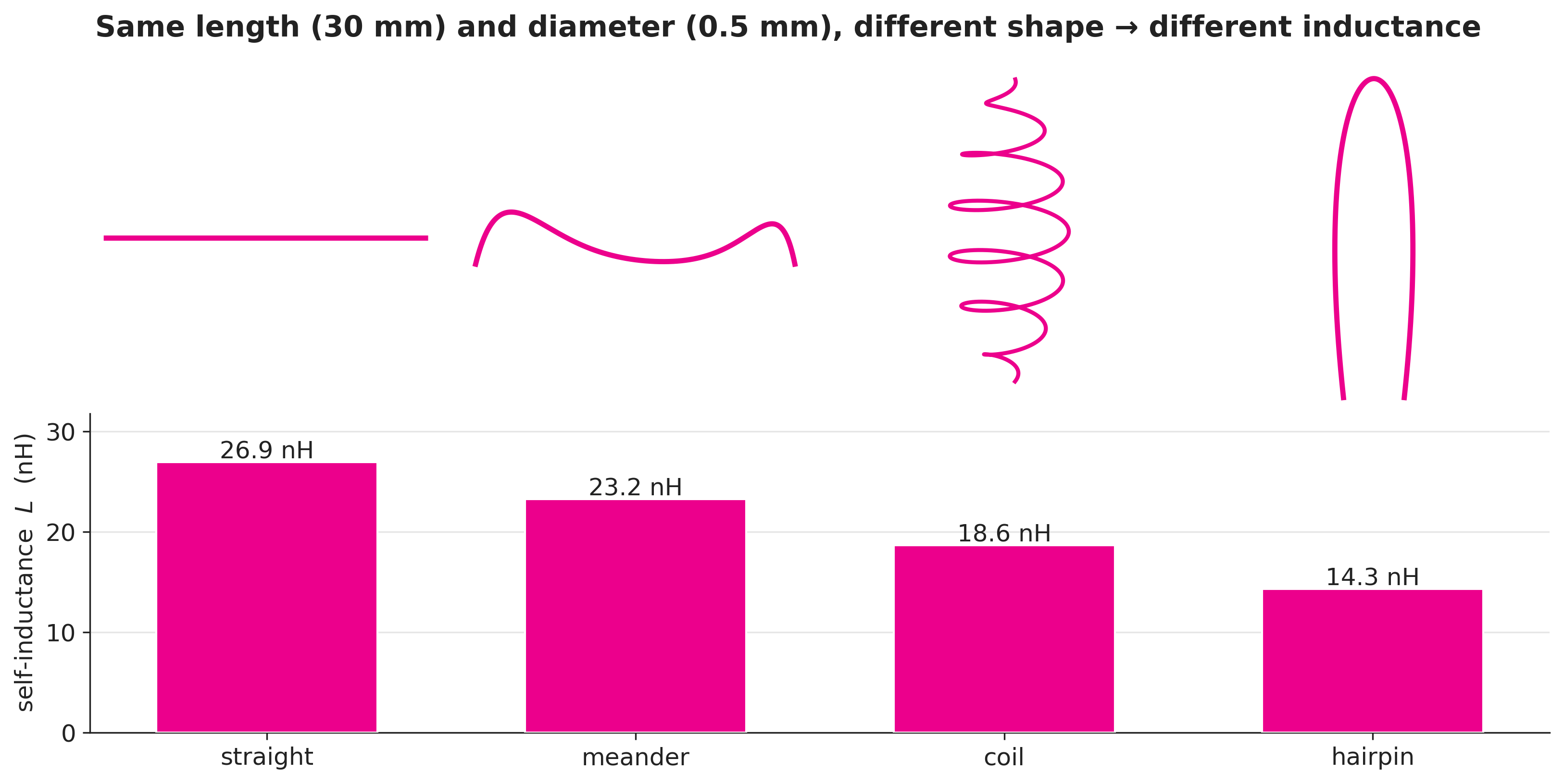 Fig. 15.: Same length (30 mm) and diameter, four different shapes, four different inductances (computed with the Neumann library).
What about the ground plane? A wire above ground has a return current flowing in the opposite direction underneath it, which lowers the effective inductance. The clean way to handle this is the method of images: replace the ground plane with a mirror-image wire carrying the opposite current, and the effective loop inductance becomes
\[L_W = L - M, \label{eq:10}\]where $L$ is the wire’s self-inductance and $M$ is the mutual inductance with its image.
As a concrete check, a symmetric 573.9 µm Bézier wirebond sitting 200 µm above a ground plane works out to $L = 380\,\mathrm{pH}$ and $M = 41\,\mathrm{pH}$, so $L_W = L - M = 339\,\mathrm{pH}$ (the ground plane shaves off about 40 pH). Adding the distributed capacitance to ground and building a lumped Π-model from these values, the S-parameters match the EM simulation almost perfectly.
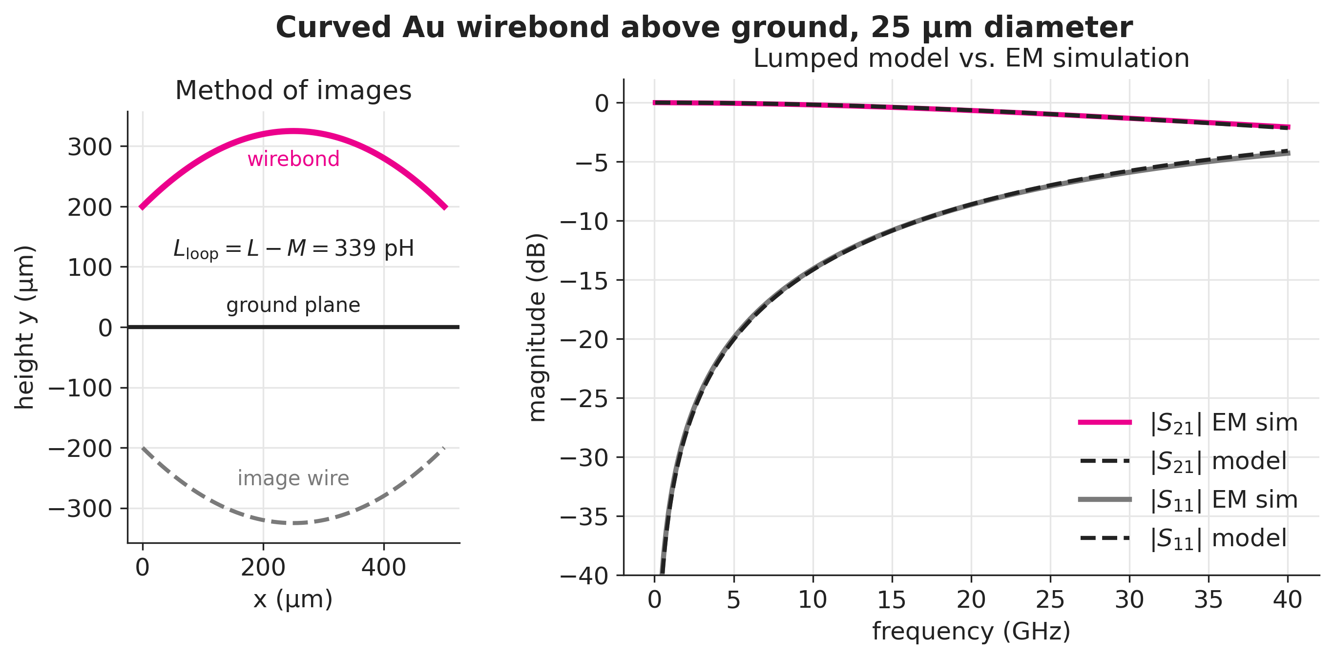 Fig. 16.: Left: the ground plane replaced by a mirrored image wire. Right: the resulting lumped model versus the EM simulation.
The GSG Case
For GSG wirebonds we combine three wires. Each wire has its own self-inductance and mutual inductance to the others, and we wire them up in the GSG topology. Applying Kirchhoff’s laws to that network, and using symmetry between the two ground wires, the net inductance works out to [6]
\[L_\mathrm{net} = L_1 - M_{12} + \frac{L_2 + M_{23} - M_{12} - M_{13}}{2} + \frac{(M_{12} - M_{13})(L_2 - M_{12} - M_{23} + M_{13})}{2(L_2 - M_{23})}, \label{eq:11}\]where subscript 1 is the signal wire and 2, 3 are the grounds. Every $L$ and $M$ in there comes straight from the Neumann integrals above.
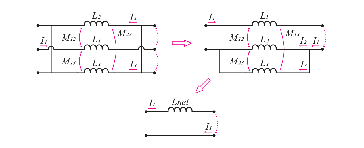 Fig. 17.: Reducing the three coupled GSG inductors to a single net inductance.
The payoff is in the next plot, which compares the loop inductance of a GSG wirebond against a single wire sitting above a ground plane at different heights. A 100 µm-pitch GSG bond matches a wire only 100 µm above ground, and it stays low no matter how thick the chips are, because the return path (the ground wires) always stays right next to the signal wire. A wire over a ground plane, by contrast, gets worse as the chip gets thicker and lifts it away from ground.
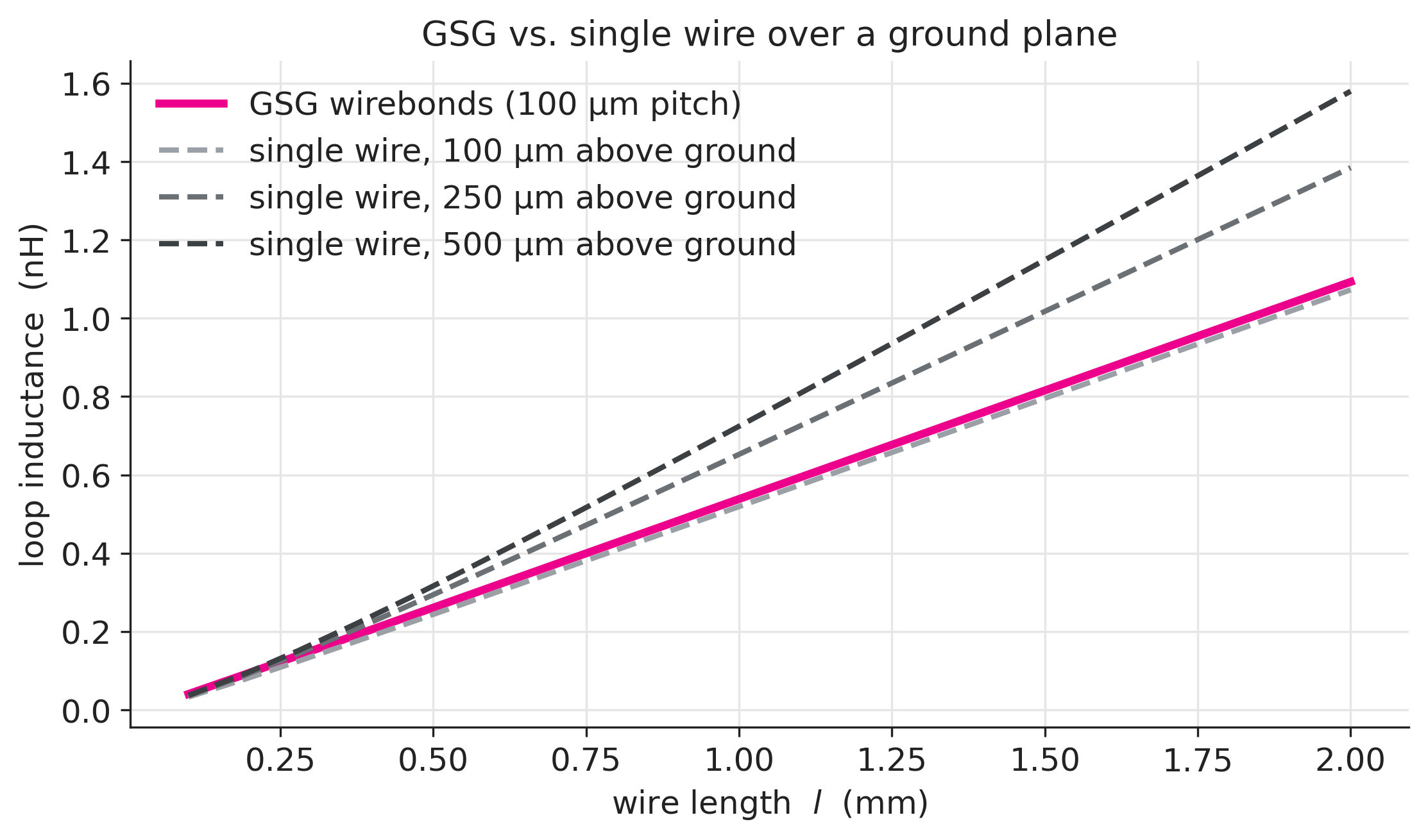 Fig. 18.: Loop inductance of GSG wirebonds versus a single wire above ground, as a function of length. The GSG curve tracks the 100 µm-above-ground case and stays there regardless of chip thickness.
GSG as a Transmission Line
Inductance is only a problem when the wires act as lumped elements in a mismatched configuration. But if the GSG wires run roughly parallel and uniform, they form a little coplanar waveguide in the air, so we can treat them as a transmission line with a characteristic impedance [11]. Goossen gives a handy closed-form approximation for this coplanar case [5]:
\[Z_0 \approx \frac{140}{\sqrt{\epsilon_\mathrm{eff}}}\,\frac{s/d - 1}{1 + 0.6(s/d - 1)}, \qquad 2 < s/d < 10, \label{eq:12}\]where $s$ is the wire-to-wire pitch, $d$ is the wire diameter, and $\epsilon_\mathrm{eff}$ is the effective relative permittivity of whatever surrounds the wires. Plug in my numbers, $d = 25\,\mu\mathrm{m}$ and $s = 100\,\mu\mathrm{m}$ in air ($\epsilon_\mathrm{eff} = 1$), and you get $Z_0 \approx 150\,\Omega$. That is high, which makes sense because wirebonds are more inductive than capacitive, but it is a serious mismatch for a 50 Ω chip. The equation gives us three parameters to lower it: reduce the pitch $s$, increase the diameter $d$ (weak effect, and limited by pad size), or raise $\epsilon_\mathrm{eff}$. The plot below puts the interesting combinations together.
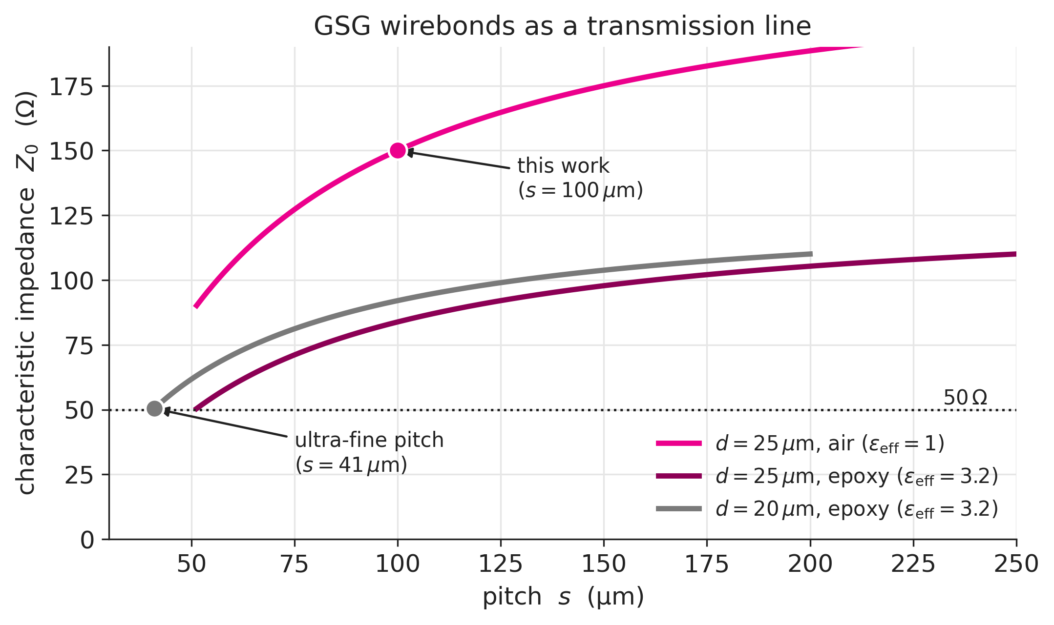 Fig. 19.: The parameters for lowering $Z_0$ (Eq. \eqref{eq:12}): pitch, diameter, and the surrounding dielectric. My wirebonds sit at 150 Ω; an ultra-fine-pitch bond covered in epoxy reaches 50 Ω.
The dielectric deserves a closer look, because it is the one you can apply after bonding: cover the wires with an epoxy (a “glob-top” in packaging terms), and the extra permittivity raises the distributed capacitance without touching the inductance. In an EM simulation from my thesis (0.5 mm long bonds, epoxy with $\epsilon_r = 3.2$), coating GSG wirebonds tripled their capacitance and pulled $Z_0$ from 155 Ω down to 89 Ω, improving the reflection from −7.9 to −10.3 dB. The same trick on GSG ribbon bonds went from 108 Ω to 62 Ω (−11.7 to −18.7 dB reflection), confirming once more that ribbons plus a dielectric coating is about the best you can do with bonded interconnects [1]. And none of the numbers in the plot are hypothetical: ultra-fine-pitch wedge tools (35 µm pitch with 20 µm wire) and chip-packaging epoxies with exactly these permittivities are off-the-shelf products.
From Theory to Practice
Enough theory. Do real wirebonds actually behave like the models say? To find out, I built and measured a set of GSG wirebonds. The test vehicles were two 750 µm-thick passive silicon interposers with 400 µm-long aluminum GSG pads at 100 µm pitch. I glued pairs of interposers onto a carrier PCB (with alignment markings), faced their GSG pads toward each other, and bonded them with 25 µm gold wire using the wedge tool. By varying the gap between the chips I got a whole range of wire lengths.
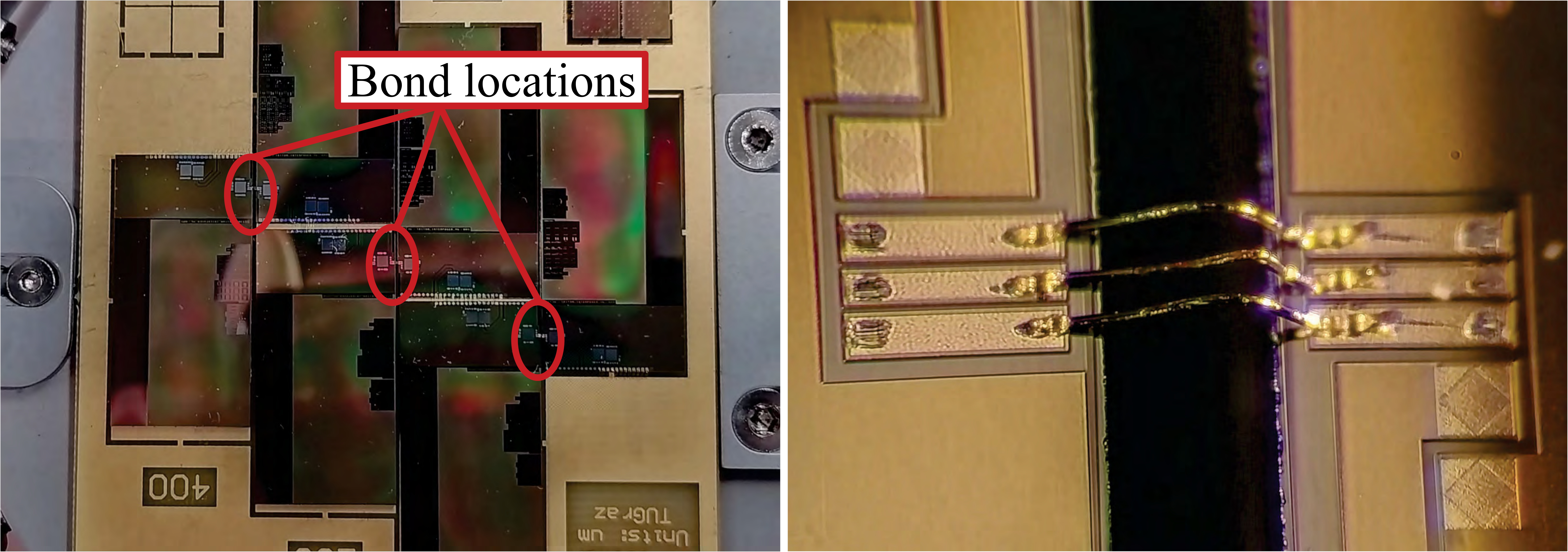 Fig. 20.: Left: interposer pairs glued on the carrier PCB (the “Bond locations” are the GSG pad sets). Right: a zoomed view of one GSG wirebond bridging two chips.
The measurement itself was done on a wafer probe station: a pair of 100 µm-pitch GSG probes landing on the chip pads, connected to a VNA and calibrated up to 40 GHz with a standard SOLT calibration on an impedance standard substrate. Working a probe station was another first for me during the thesis, and landing 100 µm-pitch probe tips on tiny aluminum pads takes almost as much patience as the bonding itself. Here is the setup, with a close-up of the probes in contact:
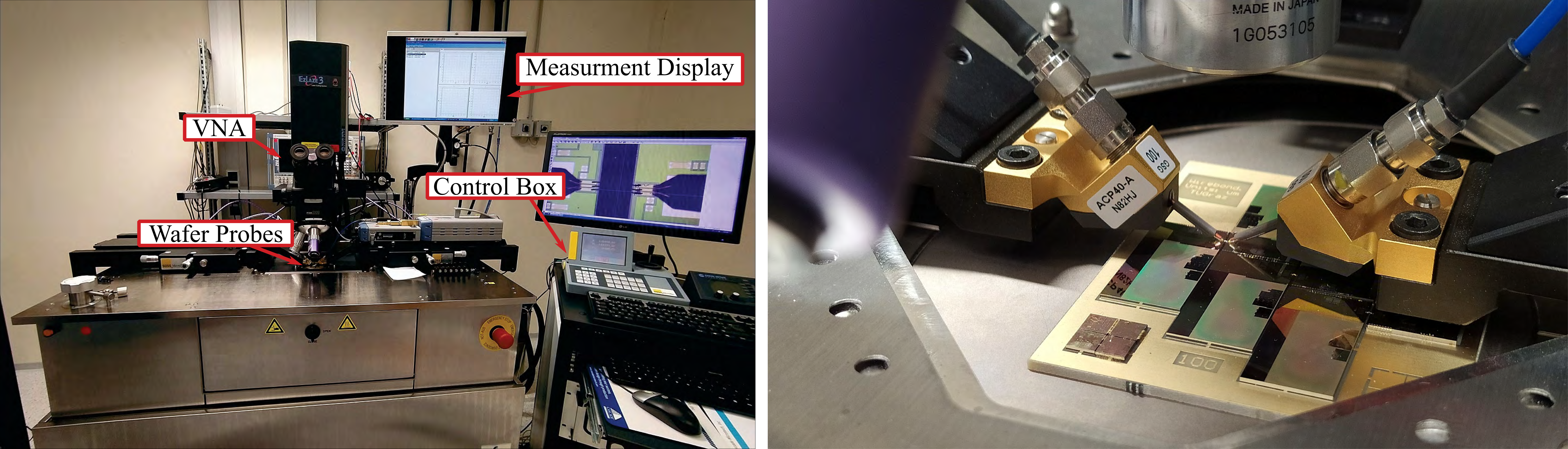 Fig. 21.: Left: the wafer probe station. Right: the GSG probes landed on the bonded chips.
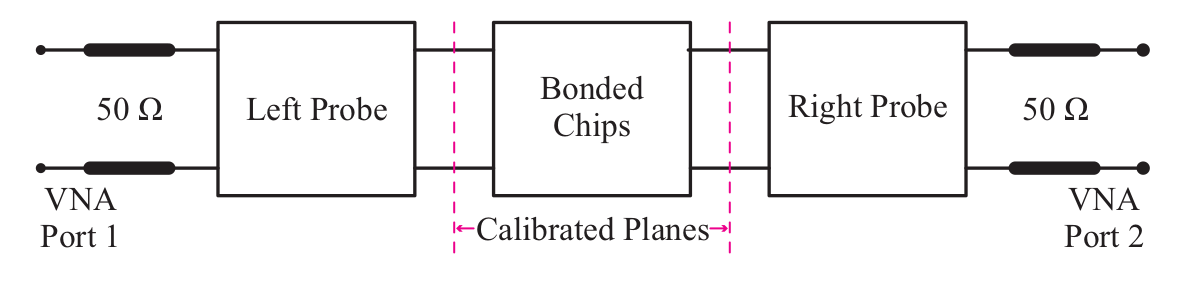 Fig. 22.: Measurement setup. The calibration planes sit at the probe tips, so the raw measurement includes the pads.
De-embedding the Pads
Here is the catch that the setup above hints at: when I probe the structure, I am not measuring only the wirebonds, I am measuring the wirebonds plus the two sets of bond pads. And the pads are not innocent bystanders. Mine were 400 µm long and built from four stacked metal layers tied together with a massive number of µ-vias (necessary so the pad survives the bonding force), and all that metal over the oxide made them surprisingly lossy. To get the wirebond by itself, I need to de-embed the pads. Because all the pads are identical, it is enough to measure one set of them without any wires attached:
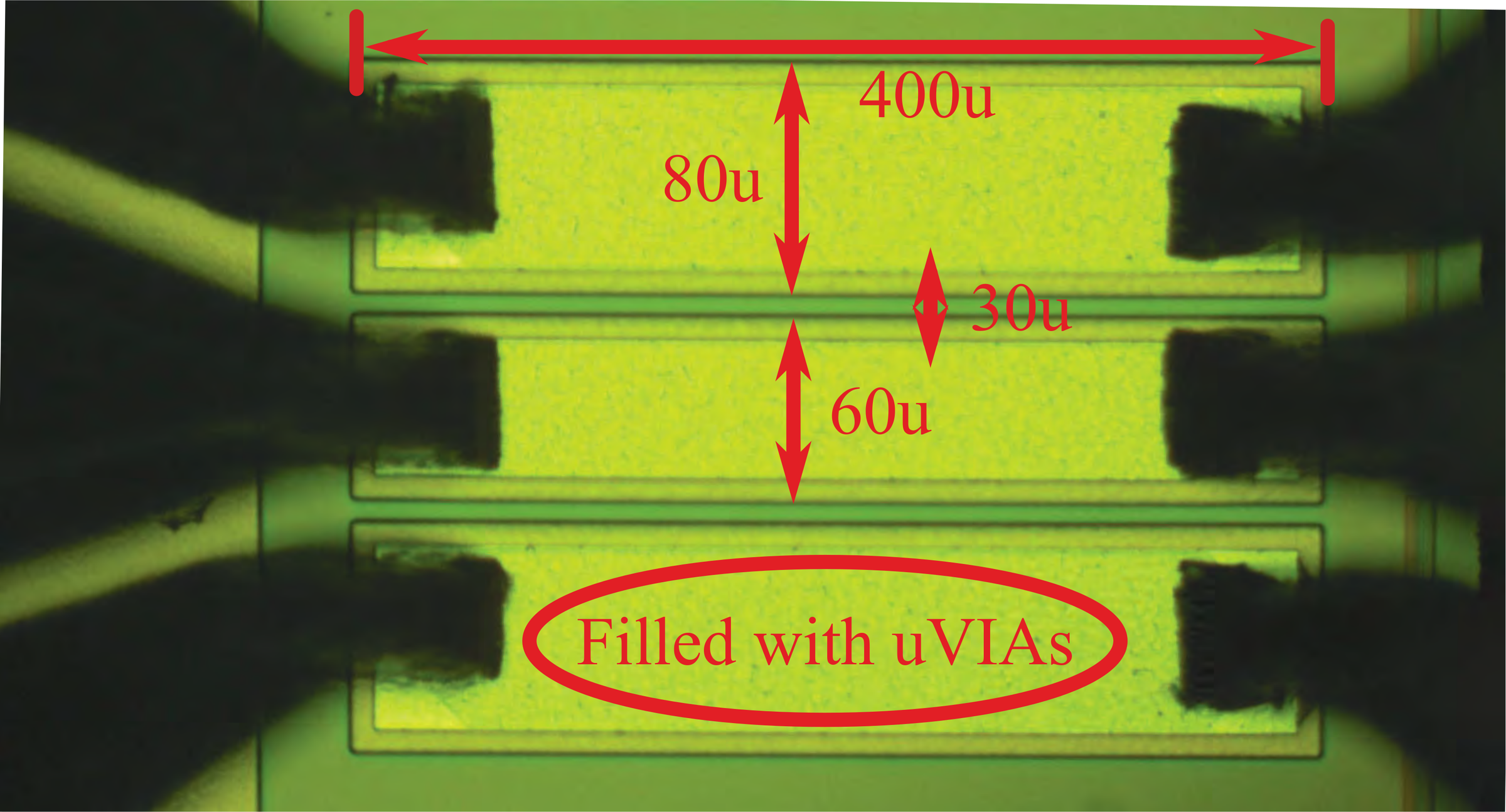 Fig. 23.: The bare GSG pads, measured separately for de-embedding. The pads are filled with µ-vias to withstand bonding, which is also what makes them lossy.
The trick is to convert the measured S-parameters into T-parameters, which cascade by simple matrix multiplication [13]. If the measurement is the left pad, then the wirebond, then the right pad, all in series, then
\[\mathbf{T}_\mathrm{Meas} = \mathbf{T}_\mathrm{L}\,\mathbf{T}_\mathrm{DUT}\,\mathbf{T}_\mathrm{R} \quad\Longrightarrow\quad \mathbf{T}_\mathrm{DUT} = \mathbf{T}_\mathrm{L}^{-1}\,\mathbf{T}_\mathrm{Meas}\,\mathbf{T}_\mathrm{R}^{-1}, \label{eq:13}\]where $\mathbf{T}_\mathrm{L}$ and $\mathbf{T}_\mathrm{R}$ are the T-parameters of the left and right pads (measured separately) and $\mathbf{T}_\mathrm{DUT}$ is what we want, the bare wirebond. One practical wrinkle: because the pad measurement is never perfect (the probe never lands on the exact same spot), de-embedding can leave the result slightly non-passive, i.e., appearing to produce a tiny bit of energy. That is easy to fix by restoring passivity with a singular value decomposition method [8], which is exactly what I did for the paper [2]: after the correction, $\lvert S_{21}\rvert$ stays at or below 0 dB everywhere, loss only, as physics demands.
Extracting the Circuit Model
With clean, de-embedded wirebond measurements in hand, the last step is to fit a lumped circuit model to them. For GSG wirebonds up to 40 GHz, a simple Π-model turned out to be enough: a series resistance $R_W$ and inductance $L_W$ in the middle, with a small capacitor to ground at each end.
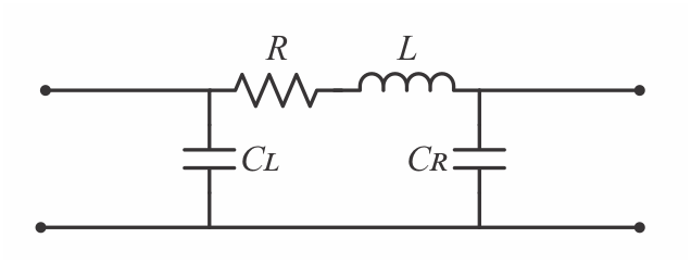 Fig. 24.: The Π-model used for the GSG wirebonds.
Finding the element values is an optimization problem: pick the parameters $\mathbf{p} = [C_L, R_W, L_W, C_R]$ that make the model’s S-parameters match the measured ones as closely as possible, by minimizing the squared error across all frequencies,
\[E(f, \mathbf{p}) = \frac{1}{N^2}\sum_{i=1}^{N}\sum_{j=1}^{N} \left|S_{ij,\mathrm{Meas}}(f) - S_{ij,\mathrm{Model}}(f, \mathbf{p})\right|^2. \label{eq:14}\]A good practical recipe is to start with a global, non-gradient optimizer (like differential evolution) to get close to the right answer without getting stuck in a bad local minimum, then switch to a fast gradient-based optimizer to polish it; that is how I ran the fits at the time. Here is one of the shorter wirebonds, showing the passivity-enforced measurement against the fitted model, both from the paper [2]:
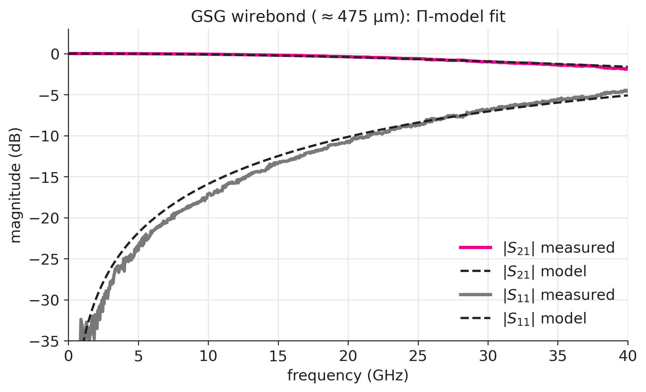 Fig. 25.: Measured (solid, passivity-enforced) versus fitted Π-model (dashed) S-parameters of a GSG wirebond around 475 µm long. The fit gives $L_W \approx 321\,\mathrm{pH}$ (data from [2]).
The agreement is excellent. Across all the shorter wirebonds (<1.2 mm) the residual fitting error stayed below −50 dB at every frequency. The simple Π-model only starts to drift from the measurements for the longest wires at the highest frequencies, where transmission-line effects kick in and you would want to cascade a couple of these sections instead [2].
The real test is whether the extracted inductances agree with the model I built in the first half of this post. In the thesis I compared them against a straight-wire approximation, which is only fair for the shortest bonds. Since then I redid it properly with the Bézier-loop model: for each span, I arch a quadratic Bézier over the gap (assuming a typical loop height) and compute the net GSG inductance with the Neumann integral. The result below tracks the measured points across the whole range, not just the short end:
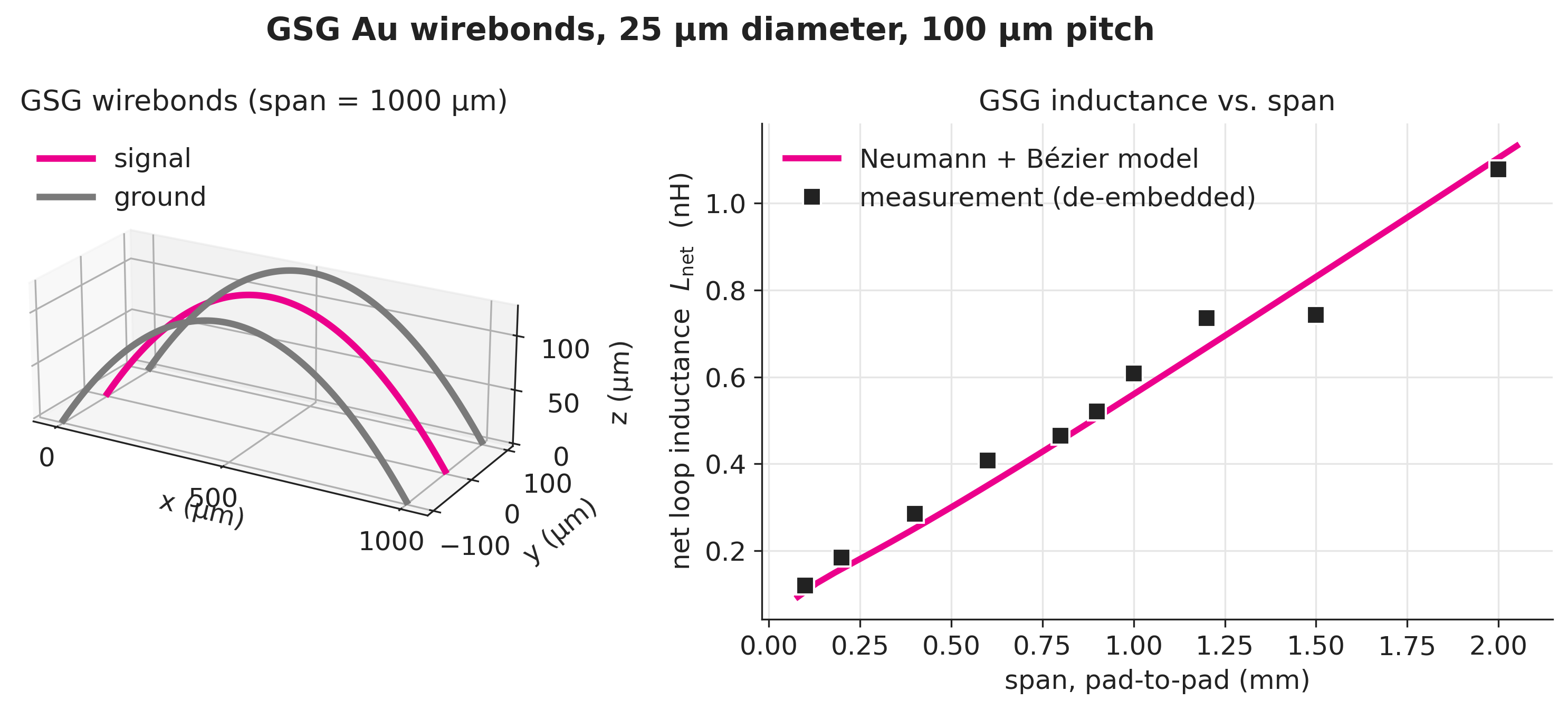 Fig. 26.: Extracted net inductance versus span. The magenta curve is the Bézier-loop model evaluated with the Neumann integral; the squares are the passivity-enforced de-embedded measurements from [2].
In the end, the GSG wirebonds shorter than 500 µm kept their insertion loss below 2 dB all the way up to 40 GHz [2]. For a manual, semi-automatic wedge bonding job, that is a genuinely good interconnect, and there is still headroom to do better with tighter pitch, ribbon bonds, or the epoxy trick from earlier.
Final Remarks
If I compress everything above into a few takeaways:
A wirebond is basically a series inductor, and at mmWave frequencies that inductance is the whole story. Keep the wires as short as possible; it is by far the biggest lever you have.
When you cannot go shorter, change the geometry. GSG wirebonds give a low loop inductance that, unlike a wire over a ground plane, does not care how thick your chips are. Ribbon bonds do even better thanks to their larger surface area.
When the geometry is also maxed out, change the surroundings: covering the wires in epoxy raises their capacitance and pulls the characteristic impedance toward 50 Ω.
You can predict all of this before touching a bonder: describe the loop with a Bézier curve, compute the inductance with the Neumann integral, and the analytical numbers match both EM simulation and real measurements remarkably well.
There is a lot more to explore that I did not cover here. And people are still actively stretching how far wirebonds can go in frequency. Recent work from KIT combined ingredients similar to the ones discussed in this post, a multi-wire coplanar arrangement with fine-tuned impedance plus a dielectric covering (a shaped adhesive film in their case), and demonstrated bond-wire interconnects running from DC to 210 GHz [14] and even 300 GHz [15] with around 1 dB of insertion loss. It is genuinely satisfying to see the concepts I played with in my thesis pushed to sub-THz. But the thing I keep coming back to is the human side of it. For all the math, modeling, and analysis in this post, a huge amount of RF wirebonding still comes down to a person with steady hands, good tools, and a lot of patience. So the next time you hear that a chip is connected by wires “thinner than a human hair,” maybe give a small nod to whoever threaded that wire through the tool 😉.
References
[1] Z. Hatab, “Realization and verification of wirebond interconnects for heterogeneous 2.5D integration of RF chips,” M.Sc. thesis, Graz Univ. of Technol., Graz, Austria, 2020, doi: 10.3217/jsfta-mfn38.
[2] Z. Hatab, E. Leitgeb, and M. E. Gadringer, “Broadband characterization of co-planar GSG wirebonds for RF heterogeneous 2.5D integration,” in 2021 97th ARFTG Microwave Measurement Conference (ARFTG), 2021, doi: 10.1109/ARFTG52261.2021.9640137.
[3] C. R. Paul, Inductance: Loop and Partial. Hoboken, NJ: Wiley-IEEE Press, 2010, ISBN: 9780470461884.
[4] Bond Wire Modeling Standard, EIA/JEDEC Standard JESD59, Jun. 1997.
[5] K. W. Goossen, “On the design of coplanar bond wires as transmission lines,” IEEE Microwave and Guided Wave Letters, vol. 9, no. 12, pp. 511-513, Dec. 1999, doi: 10.1109/75.819415.
[6] X. Qi, “High frequency characterization and modeling of on-chip interconnects and RF IC wire bonds,” Ph.D. dissertation, Stanford University, Stanford, CA, 2001.
[7] T. Krems, W. Haydl, L. Verweyen, M. Schlechtweg, H. Massler, and J. Rüdiger, “Coplanar bond wire interconnections for millimeter-wave applications,” in Proc. Electrical Performance of Electronic Packaging, Portland, OR, USA, 1995, pp. 178-180, doi: 10.1109/EPEP.1995.524887.
[8] E. D. Campbell, A. Morales, and S. Agili, “A simple method for restoring passivity in S-parameters using singular value decomposition,” in 2010 Digest of Technical Papers Int. Conf. on Consumer Electronics (ICCE), Las Vegas, NV, USA, 2010, pp. 219-220, doi: 10.1109/ICCE.2010.5418695.
[9] G. Harman, Wire Bonding in Microelectronics, 3rd ed. New York, NY: McGraw-Hill, 2010, ISBN: 9780071476232.
[10] S. K. Prasad, Advanced Wirebond Interconnection Technology. New York, NY: Springer, 2006.
[11] R. H. Caverly, “Characteristic impedance of integrated circuit bond wires,” IEEE Transactions on Microwave Theory and Techniques, vol. 34, no. 9, pp. 982-984, Sep. 1986, doi: 10.1109/TMTT.1986.1133480.
[12] I. J. Bahl, Lumped Elements for RF and Microwave Circuits. Norwood, MA: Artech House, 2003, ISBN: 9781580533096.
[13] D. A. Frickey, “Conversions between S, Z, Y, H, ABCD, and T parameters which are valid for complex source and load impedances,” IEEE Transactions on Microwave Theory and Techniques, vol. 42, no. 2, pp. 205-211, Feb. 1994, doi: 10.1109/22.275248.
[14] L. Valenziano, J. Hebeler, G. Gramlich, A. Quint, T. Zwick, and A. Bhutani, “Advanced bond-wire interconnect solution for ultra-broadband applications covering DC to 210 GHz,” IEEE Transactions on Components, Packaging and Manufacturing Technology, vol. 14, no. 11, pp. 1921-1930, Nov. 2024, doi: 10.1109/TCPMT.2024.3465608.
[15] L. Valenziano, J. Hebeler, Y. Bao, C. Koos, T. Zwick, and A. Bhutani, “A 300 GHz bond-wire interconnect solution for heterogeneous system integration,” in 2025 55th European Microwave Conference (EuMC), Utrecht, Netherlands, 2025, pp. 69-72, doi: 10.23919/EuMC65286.2025.11235147.